

Comprehensive Guide to Wafer Probe Testing: Critical Process in Semiconductor Manufacturing
1. Introduction to Wafer Probe Testing
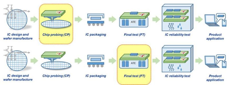
Wafer Probe Testing (also known as Chip Probing, CP) is a pivotal step in semiconductor manufacturing, performed after wafer fabrication but before chip packaging. This process electrically validates each die (individual chip unit) on the wafer to identify defects early, thereby reducing packaging costs and improving yield. With the rise of advanced nodes (5nm and below) and heterogeneous integration (e.g., 3D ICs, Chiplets), wafer probe testing has evolved into a highly sophisticated process requiring nanometer-level precision and cutting-edge probe technologies.
2. Technical Workflow of Wafer Probe Testing
2.1 Key Stages of Wafer Probe Testing
1.Wafer Loading:
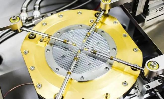
The wafer is mounted on a prober (wafer handling system) with sub-micron alignment accuracy.
Vacuum chucks stabilize the wafer to prevent mechanical shifts during testing.
2.Wafer Probe Contact:
A probe card with micro-scale needles (probe pins) makes direct electrical contact with the die’s pads or bumps.
Advanced probe cards (e.g., MEMS-based) achieve contact forces as low as 0.1g to avoid pad damage.
3.Electrical Testing:
Automated Test Equipment (ATE) applies test signals (voltage, current, digital patterns) to validate functionality and parametric performance.
Critical tests include continuity checks, IDDQ leakage tests, scan chain validation, and ADC/DAC linearity verification.
4.Data Analysis & Marking:
Defective dies are marked using ink dots or laser etching for post-test exclusion.
Statistical process control (SPC) tools correlate test data with wafer fabrication parameters (e.g., CMP uniformity, lithography overlay).
2.2 Role of Wafer Probe Testing in Yield Management
Cost Savings: Screening defective dies before packaging saves **2 per chip** (typical packaging cost).
Process Feedback: Wafer probe data identifies lithography or etch variations, enabling real-time fab process adjustments.
3. Wafer Probe Technologies: Innovations and Applications
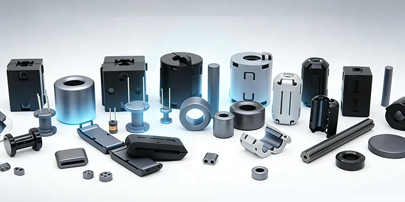
3.1 Probe Card Breakthroughs
| Type | Key Features | Applications |
| Cantilever Probe | Low cost, 50–100μm pad pitch support | Mature nodes (28nm and above) |
| Vertical Probe | High-density (20–50μm pitch), multi-DUT testing | 3D ICs, HBM memory |
| MEMS Probe Card | Ultra-fine pitch (<10μm), 67GHz RF testing capability | 5G mmWave, AI/ML chips |
| Photon Probe | Non-contact optical probing, zero mechanical wear | GaN/SiC power devices, R&D applications |
3.2 Emerging Wafer Probe Testing Trends
AI-Driven Optimization: Machine learning algorithms predict probe card wear, reducing downtime by 30%.
Multi-Site Parallel Testing: 512–1,024 dies tested simultaneously via high-pin-count ATE systems.
High-Temperature Wafer Probe Testing: Thermal chucks enable testing at **-55°C to 300°C** for automotive-grade ICs.
4. Wafer Probe Testing in Advanced Packaging
4.1 Challenges for Heterogeneous Integration
TSV (Through-Silicon Via) Testing: Wafer probe systems must validate TSV resistance (<0.1Ω) and capacitance uniformity.
Chiplet Interconnect Validation: Probe cards with μbump-compatible tips test microbump arrays (10–20μm pitch) in 2.5D/3D packages.
4.2 Case Study: Wafer Probe Testing for HBM4
Test Requirements:
8-Hi stack validation (1024 data channels).
6.4Gbps/pin signal integrity at 1.0V.
Solution:
MEMS probe cards with **<5ps skew** and **>56GHz bandwidth**.
Adaptive voltage scaling (AVS) during testing to mimic real-world workloads.
5. Economic Impact of Wafer Probe Testing
Cost Breakdown:
Probe Card: 500k (depending on technology).
ATE Utilization: 800/hour (e.g., Advantest V93000).
ROI Optimization:
Reducing test time per die by 0.5 seconds saves **10M annually** for a high-volume fab.
Probe card refurbishment programs cut replacement costs by 40–60%.
6. Future Directions in Wafer Probe Testing
Quantum Computing ICs: Cryogenic wafer probe systems operating at 4K (–269°C) for qubit validation.
Photonics Integration: Co-testing optical and electrical interfaces in silicon photonics devices.
Sustainable Practices: Recycling tungsten probe needles and lead-free PCB materials.
Shenzhen Gaorunxin Technology Co., Ltd