How to Choose Copper Thickness and Trace Width in PCB Design?
In PCB design, copper thickness and trace width are two critical parameters that significantly impact the performance and functionality of the circuit board. Here are some guidelines on selecting copper thickness and trace width for PCB design:
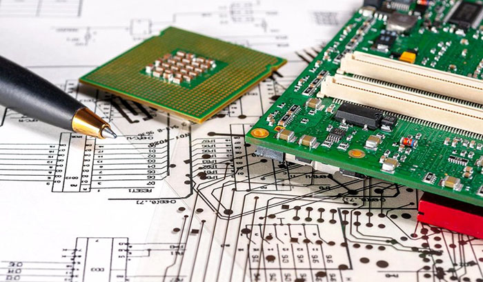
Copper Thickness Selection: Copper thickness refers to the thickness of the copper foil on the PCB, typically measured in ounces (oz). Common options include 1oz, 2oz, and 3oz. A higher copper thickness provides better current-carrying capacity and thermal conductivity but increases cost and board weight. The choice should be based on power requirements, trace width/spacing needs, and other design considerations.
Trace Width Selection: Trace width refers to the width of conductive paths on the PCB, usually measured in millimeters or inches (e.g., 0.2mm, 8mil). The selection depends on power demands, signal frequency, impedance control, and manufacturing constraints. Wider traces improve current handling and reduce resistance, while narrower traces enable higher routing density and finer layouts.
Relationship Between Trace Width and Copper Thickness: Trace width and copper thickness are interrelated. Thinner copper allows for narrower traces, while thicker copper requires wider traces to ensure uniform current distribution, minimize impedance, and prevent heat buildup.
Manufacturing Capability and Cost: When selecting trace width and copper thickness, consider the PCB manufacturer's capabilities and cost constraints. Some factories may have limitations on extremely fine traces or thick copper layers. Additionally, these choices affect PCB cost due to material usage, fabrication complexity, and processing time.
To make the right choice, evaluate circuit requirements, power needs, signal characteristics, manufacturing feasibility, and budget. Before finalizing the design, consult your PCB manufacturer to confirm their capabilities and recommended ranges for trace width and copper thickness.
Shenzhen Gaorunxin Technology Co., Ltd


