

What is a Crystal Oscillator?
As the core component in digital circuit design, crystal oscillators act as the "heart" of electronic systems. All digital circuits rely on clock signals, and crystal oscillators precisely control system initialization. Wherever digital circuits exist, crystal oscillators are indispensable.
1. What is a Crystal Oscillator?
Crystal oscillators refer to quartz crystal resonators and oscillators. Both utilize the piezoelectric effect of quartz crystals. When voltage is applied to the crystal's electrodes, mechanical deformation occurs. Conversely, mechanical stress generates an electric field. This reversible phenomenon allows crystals to vibrate and generate alternating electric fields when AC voltage is applied. Although these vibrations are typically weak, they exhibit significant resonance amplification at specific frequencies, similar to LC circuit resonance.
2. Types of Crystal Oscillators (Passive vs. Active)
① Passive Crystal Oscillators
- 2-pin devices (some with fixed non-polar pins)
- Require external load capacitors to generate sine wave signals
- Depend on circuit configuration for oscillation
② Active Crystal Oscillators
- 4-pin self-contained oscillators
- Generate square waves independently
- Offer higher stability (±5ppm), simpler implementation, but higher cost
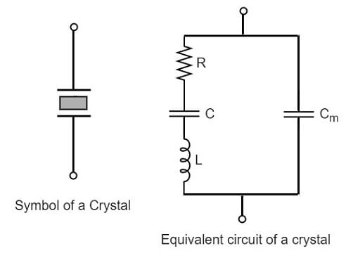
3. Equivalent Circuit Model
A crystal oscillator behaves like a series RLC circuit paralleled with a capacitance (Cm):
- Non-vibrating state: Acts as capacitor Cm
- Vibrating state: Functions as tuned RLC circuit
- Operates at series resonance frequency
4. Key Parameters
- Frequency: Ranges from 4MHz to 100MHz+ (MCU-dependent)
- Accuracy: ±5ppm to ±50ppm (high-precision chips use ±5ppm)
- Load Capacitance: Adjustable for frequency tuning
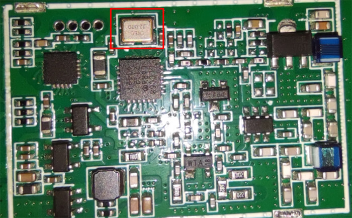
5. PCB Layout Guidelines
As critical components, improper crystal oscillator placement causes system instability and EMI issues. Key layout principles:
① Edge Proximity Avoidance
- Minimum 300mil from PCB edges
- Encase with ground traces/vias if edge placement is unavoidable
- Always ground metal casing to suppress radiation
② Signal Isolation
- No signal traces under oscillator area
- Maintain clear zone within 300mil radius
③ Component Arrangement
- Place filter capacitors near power pins
- Arrange components along signal flow path
- Keep matching networks close to MCU
④ Clock Routing
- Short, wide traces with priority routing
- Balance between trace length and heat source distance
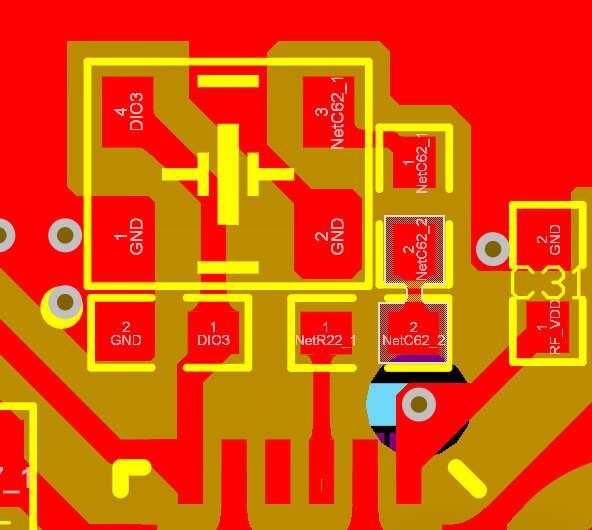
Recommended Layout Example:
- Cluster oscillator, capacitors, and MCU compactly
- Straight short traces to MCU clock pins
- Ground shielding around oscillator
High-frequency clock signals (especially >50MHz) require strict layout control. Improper placement causes strong harmonic radiation that's difficult to mitigate post-production. Always prioritize oscillator and clock signal routing in PCB design.
Shenzhen Gaorunxin Technology Co., Ltd