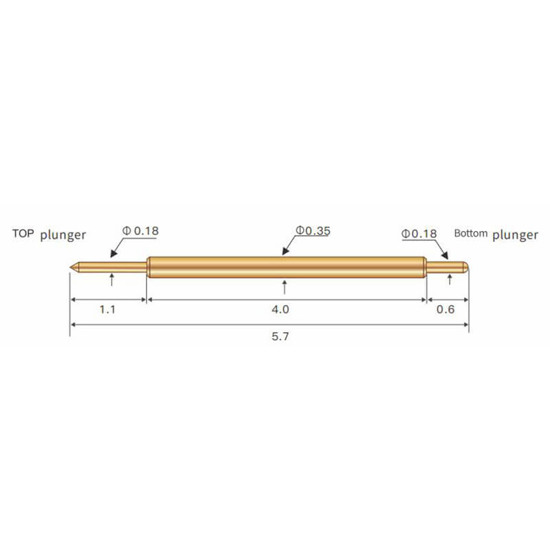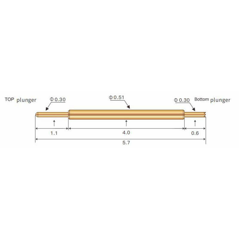


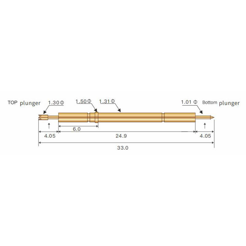
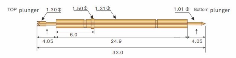
24.9mm Semiconductor Test Probe| 1.311mm dia 1A | Used Test Wafer
- Product Name: Semiconductor Test Probe
- Catalog Number: DE1-131FB330-01C0
- Current Rating: 2A
- Contact Resistance: 200 mohms max
- Bandwidth: [email protected]
- Inductace: 2.02nH
- Captance: 3.44pF
- Product Details
- Download
Semiconductor test probes are precision components specifically designed for integrated circuit (IC) verification across multiple critical stages.
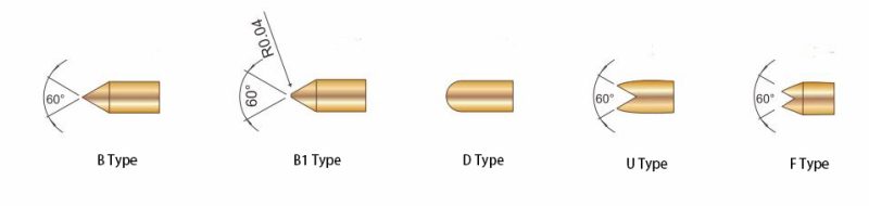
Probe Tips
Material Plated:
Barrel:Brass / Gold Plated
Bottom:SK4(Be Cu)/Gold Plated
TOP:SK4(Be Cu)/Gold Plated
Spring:SWPB(SUS)/Gold Plated
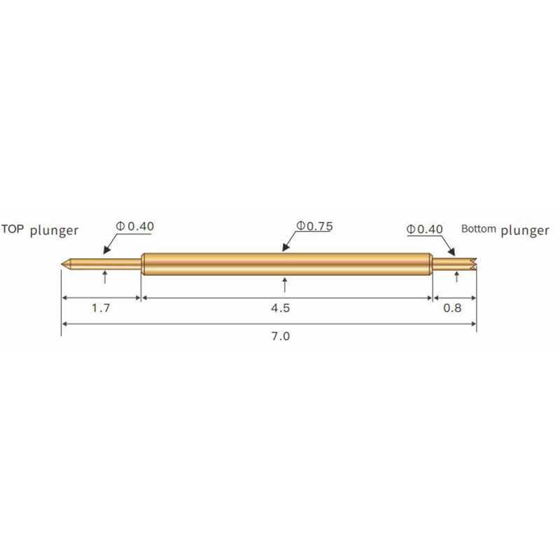
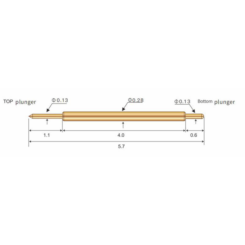
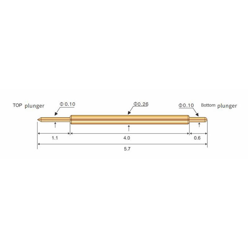
Specification:
Full Stroke:6.0mm
Rated Stroke:2.0mm
Spring Force:[email protected]
Mechanical Life Exceeds:200K
Key applications include:
IC functional/parametric testing
Microneedle module burn-in & aging validation
Open/short circuit diagnostics
High-speed data communication signal integrity analysis
Technical Specifications:
Pitch compatibility: 0.3mm, 0.4mm, 0.5mm, 0.65mm, 0.75mm, 1.0mm, 1.27mm, 2.54mm
Probe configuration: Customizable based on test socket specifications
Frequency range: 5G-40G (DC to 40 GHz RF capability)
Performance characteristics: <0.5ohm contact resistance, <1dB insertion loss
Industry Applications:
Consumer electronics (mobile devices, computing systems)
Advanced connectivity solutions (high-end connectors, backplane interconnects)
Communication infrastructure (5G base stations, optical modules)
Emerging technologies (AI accelerators, automotive electronics)
These probes demonstrate exceptional performance in semiconductor wafer testing and advanced packaging validation, particularly in high-density probing scenarios requiring ultra-low contact resistance and multi-gigabit signal transmission stability.
Shenzhen Gaorunxin Technology Co., Ltd
Online message
Shenzhen Gaorunxin Technology Co., Ltd