

CRSM650N20N3Z CR Micro 200V 19A N-Channel MOSFET PDFN5×6
- Product Details
- Download
- 200 V / 19 A continuous drain current, PDFN5×6 package
- Rds(on) 57 mΩ typ, 65 mΩ max at VGS = 10 V
- Qg 13 nC and Ciss 834 pF
- N-channel, SGT process
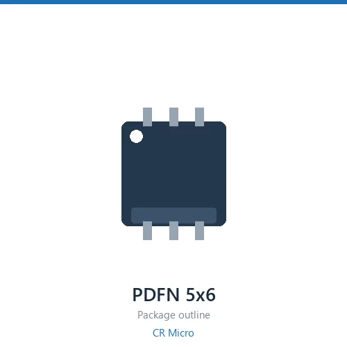
The CR Micro CRSM650N20N3Z is a 200 V 19 A N-channel MOSFET in a PDFN5×6 package, built on the SGT process. On-resistance is 57 mΩ typical and 65 mΩ maximum at a 10 V gate drive; gate charge is 13 nC with 834 pF input capacitance; threshold voltage spans 2 to 4 V.
Key Specifications
| Drain-Source Voltage (VDS) | 200 V |
| Continuous Drain Current (ID) | 19 A |
| Rds(on) @ VGS = 10 V, typ. | 57 mΩ |
| Rds(on) @ VGS = 10 V, max. | 65 mΩ |
| Gate Threshold Voltage (VGS(th)) | 2 – 4 V |
| Total Gate Charge (Qg) | 13 nC |
| Input Capacitance (Ciss) | 834 pF |
| Channel Polarity | N-channel |
| Process Family | SGT |
| Package | PDFN5×6 |
Same-Rating Selection Table
| Part Number | VDS | ID | Rds(on) typ | Rds(on) max | Qg | Ciss | Package |
|---|---|---|---|---|---|---|---|
| CRSM420N20N3Z | 200V | 30A | 29 | 42 | 19.1 | 1206 | PDFN5×6 |
| CRSM650N20N3 | 200V | 19A | 57 | 65 | 13 | 834 | PDFN5×6 |
| CRSM650N20N3Z | 200V | 19A | 57 | 65 | 13 | 834 | PDFN5×6 |
3 part numbers share the same 200 / PDFN5×6 / N rating — sorted by rds(on) typ.
Process Technology
SGT (Shielded Gate Trench) — a trench gate with a grounded shield electrode beneath it. The shield cuts the gate-drain capacitance, so Qg and Crss drop sharply against a conventional trench at the same Rds(on). This is the workhorse process for 30–200 V and for 600–650 V high-frequency switching.
Applications
Telecom and server DC-DC stages, Class-D audio, PoE interfaces, and 48 V motor drive.
Selection Notes
- Rds(on) rises with junction temperature. Size the heatsink against the hot value given in the datasheet, not the 25 °C number in the table above.
- If the gate is driven below 10 V, check the 4.5 V Rds(on) line — parts without that rating are not characterised for logic-level drive.
- For high-frequency stages compare Qg and Ciss against the Rds(on) gain. A part one bin lower in Rds(on) often costs more switching loss than it saves in conduction.
- The body diode recovery of low-Rds(on) parts can be severe in bridge topologies. Verify dv/dt and dead time against the datasheet before dropping it into a half bridge.
Common Questions
Is the CRSM650N20N3Z an N-channel or P-channel device?
It is N-channel. The drain-source rating is 200 V.
Can the CRSM650N20N3Z be driven at 4.5 V?
No 4.5 V on-resistance figure is published for this part. It is characterised at 10 V gate drive, so use a driver that reaches 10 V.
What is the gate threshold voltage of the CRSM650N20N3Z?
VGS(th) is specified between 2 and 4 V. Below the lower figure the part is off; above the upper figure it is fully on at the rated current.
How much gate charge does the CRSM650N20N3Z need?
Qg is 13 nC. Size the driver against that figure at your switching frequency, and add the gate loop loss to the total dissipation budget.
What package does the CRSM650N20N3Z come in?
PDFN5×6. Check the datasheet mechanical drawing for lead spacing and thermal pad dimensions before laying out the footprint.
How do I choose between the 3 part numbers in this rating group?
All 3 share the same voltage and package class. Sort by on-resistance first, then check gate charge: the lowest Rds(on) part is not automatically the best choice if the stage switches at high frequency. The table above lists them in ascending Rds(on) order.
Shenzhen Gaorunxin Technology Co., Ltd
Online message
Shenzhen Gaorunxin Technology Co., Ltd