

CRXZA14M065G4Z CR Micro 750V 120A SiC MOSFET QDPAK
- Product Details
- Download
- 750 V / 120 A continuous drain current, QDPAK package
- Rds(on) 18 mΩ typ, 25 mΩ max at VGS = 15 V
- Qg 125 nC and Ciss 3127 pF
- N-channel silicon carbide, 4H-SiC
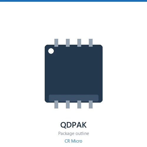
The CR Micro CRXZA14M065G4Z is a 750 V 120 A N-channel silicon carbide MOSFET in a QDPAK package. 18 mΩ typical at a 15 V gate drive (25 mΩ maximum); 14 mΩ typical at 18 V; Qg is 125 nC; VGS(th) 2 to 4 V.
Key Specifications
| Drain-Source Voltage (VDS) | 750 V |
| Continuous Drain Current (ID) | 120 A |
| Rds(on) @ VGS = 15 V, typ. | 18 mΩ |
| Rds(on) @ VGS = 15 V, max. | 25 mΩ |
| Rds(on) @ VGS = 18 V, typ. | 14 mΩ |
| Rds(on) @ VGS = 18 V, max. | 20 mΩ |
| Gate Threshold Voltage (VGS(th)) | 2 – 4 V |
| Total Gate Charge (Qg) | 125 nC |
| Input Capacitance (Ciss) | 3127 pF |
| Channel Polarity | N-channel |
| Package | QDPAK |
Same-Rating Selection Table
| Part Number | VDS | ID | Rds 15V typ | Rds 15V max | Qg | Ciss | Package |
|---|---|---|---|---|---|---|---|
| CRXZA10M065G4 | 750V | 160A | 13 | 19 | 187 | 4433 | QDPAK |
| CRXZA14M065G4Z | 750V | 120A | 18 | 25 | 125 | 3127 | QDPAK |
| CRXZA20M065G4 | 750V | 85A | 25 | 25 | 77 | 2274 | QDPAK |
| CRXZA25M065G4 | 750V | 70A | 32 | 45 | 78.4 | 1777 | QDPAK |
| CRXZA25M065G4Q | 750V | 70A | 32 | 45 | 78.4 | 1777 | QDPAK |
| CRXZA40M065G4Q | 750V | 42A | 50 | 65 | 47 | 1196 | QDPAK |
| CRXZA40M065G4Z | 750V | 42A | 50 | 65 | 47 | 1196 | QDPAK |
| CRXZA60M065G4Q | 750V | 30A | 75 | 95 | 32 | 731 | QDPAK |
8 part numbers share the same 750 / QDPAK / N rating — sorted by rds 15v typ.
Process Technology
Silicon carbide has a critical field roughly ten times that of silicon, so the drift layer can be far thinner for the same blocking voltage. The result is a much lower specific on-resistance at 1200 V and above, and a breakdown voltage that barely moves with temperature. The trade-offs are a narrower gate window and a body diode that should not carry continuous third-quadrant current.
Applications
High-voltage offline supplies, active clamp topologies, and single-stage PFC.
Selection Notes
- Silicon carbide holds a much flatter Rds(on) over temperature than silicon, but the gate window is narrow. Drive at 15–18 V on and a negative or zero volt off bias as the datasheet specifies.
- The body diode is not intended for continuous third-quadrant conduction. Where the topology requires it, check the datasheet's reverse conduction figures or add an external Schottky.
- Switching speed is limited by the gate loop, not the die. Keep the gate loop inductance low and budget for a negative turn-off spike on the gate.
- Paralleling needs matched VGS(th). Because VGS(th) spread is narrow the parts parallel well, but layout symmetry still decides current sharing.
Common Questions
Is the CRXZA14M065G4Z an N-channel or P-channel device?
It is N-channel. The drain-source rating is 750 V.
Can the CRXZA14M065G4Z be driven at 4.5 V?
No 4.5 V on-resistance figure is published for this part. It is characterised at 15 V gate drive, so use a driver that reaches 15 V.
How much gate charge does the CRXZA14M065G4Z need?
Qg is 125 nC. Size the driver against that figure at your switching frequency, and add the gate loop loss to the total dissipation budget.
What package does the CRXZA14M065G4Z come in?
QDPAK. Check the datasheet mechanical drawing for lead spacing and thermal pad dimensions before laying out the footprint.
How do I choose between the 8 part numbers in this rating group?
All 8 share the same voltage and package class. Sort by on-resistance first, then check gate charge: the lowest Rds(on) part is not automatically the best choice if the stage switches at high frequency. The table above lists them in ascending Rds(on) order.
Shenzhen Gaorunxin Technology Co., Ltd
Online message
Shenzhen Gaorunxin Technology Co., Ltd