

CS60N03AQ4-G CR Micro 30V 60A N-Channel MOSFET DFN3.3×3.3
- Product Details
- Download
- 30 V / 60 A continuous drain current, DFN3.3×3.3 package
- Rds(on) 3.6 mΩ typ, 5.5 mΩ max at VGS = 10 V
- Qg 53.5 nC and Ciss 2848 pF
- N-channel, Trench process
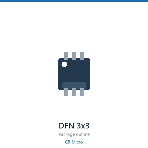
The CR Micro CS60N03AQ4-G is a 30 V 60 A N-channel MOSFET in a DFN3.3×3.3 package, built on the Trench process. On-resistance is 3.6 mΩ typical and 5.5 mΩ maximum at a 10 V gate drive; 5 mΩ typical at 4.5 V, so it also works from a logic-level driver; gate charge is 53.5 nC with 2848 pF input capacitance; threshold voltage spans 1 to 2 V.
Key Specifications
| Drain-Source Voltage (VDS) | 30 V |
| Continuous Drain Current (ID) | 60 A |
| Rds(on) @ VGS = 10 V, typ. | 3.6 mΩ |
| Rds(on) @ VGS = 10 V, max. | 5.5 mΩ |
| Rds(on) @ VGS = 4.5 V, typ. | 5 mΩ |
| Rds(on) @ VGS = 4.5 V, max. | 7.5 mΩ |
| Gate Threshold Voltage (VGS(th)) | 1 – 2 V |
| Total Gate Charge (Qg) | 53.5 nC |
| Input Capacitance (Ciss) | 2848 pF |
| Channel Polarity | N-channel |
| Process Family | Trench |
| Package | DFN3.3×3.3 |
Process Technology
Trench — the gate is etched vertically into the drift region, multiplying channel width per unit area. Lowest Rds(on) in the sub-200 V range; the trade-off is higher Qg and a more fragile body diode under hard commutation.
Applications
Low-voltage DC-DC converters, load switches, battery protection, and brushed or stepper motor drive.
Selection Notes
- Rds(on) rises with junction temperature. Size the heatsink against the hot value given in the datasheet, not the 25 °C number in the table above.
- If the gate is driven below 10 V, check the 4.5 V Rds(on) line — parts without that rating are not characterised for logic-level drive.
- For high-frequency stages compare Qg and Ciss against the Rds(on) gain. A part one bin lower in Rds(on) often costs more switching loss than it saves in conduction.
- The body diode recovery of low-Rds(on) parts can be severe in bridge topologies. Verify dv/dt and dead time against the datasheet before dropping it into a half bridge.
Common Questions
Is the CS60N03AQ4-G an N-channel or P-channel device?
It is N-channel. The drain-source rating is 30 V.
Can the CS60N03AQ4-G be driven from a 4.5 V logic-level gate signal?
Yes. The datasheet characterises Rds(on) at 4.5 V: 5 mΩ typical and 7.5 mΩ maximum.
What is the gate threshold voltage of the CS60N03AQ4-G?
VGS(th) is specified between 1 and 2 V. Below the lower figure the part is off; above the upper figure it is fully on at the rated current.
How much gate charge does the CS60N03AQ4-G need?
Qg is 53.5 nC. Size the driver against that figure at your switching frequency, and add the gate loop loss to the total dissipation budget.
What package does the CS60N03AQ4-G come in?
DFN3.3×3.3. Check the datasheet mechanical drawing for lead spacing and thermal pad dimensions before laying out the footprint.
Shenzhen Gaorunxin Technology Co., Ltd
Online message
Shenzhen Gaorunxin Technology Co., Ltd